Semiconducting materials have long been integral to the development of electronic components, with two-dimensional (2D) materials emerging as a new frontier in this field. These materials offer unique optoelectronic properties that could revolutionize the design of ultra-thin and tunable electronic devices. However, despite their potential advantages, interfacing 2D materials with gate dielectrics has posed challenges, leading to the rapid degradation of transistor performance due to interfacial traps.
Researchers from King Abdullah University of Science and Technology (KAUST), Soochow University, and other global institutes recently unveiled a novel approach that could pave the way for the fabrication of high-performance transistors based on 2D semiconductors. Their innovative design, detailed in a paper published in Nature Electronics, involves using hexagonal boron nitride (h-BN) dielectrics in conjunction with metal gate electrodes boasting a high cohesive energy.
Through their experiments, the research team discovered that employing platinum (Pt) as an anode in the h-BN stack significantly reduced the likelihood of dielectric breakdown. Subsequent tests indicated that Pt/h-BN gate stacks exhibited a 500-fold decrease in leakage current compared to Au/h-BN gate stacks, with a high dielectric strength exceeding 25 MV/cm. These results inspired the researchers to explore the use of chemical vapor deposited h-BN as a gate dielectric in 2D transistors.
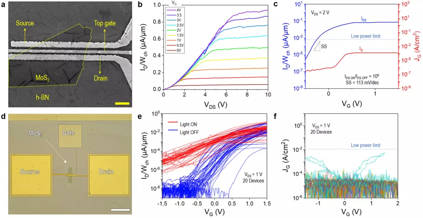
The team, led by Yaqing Shen and Prof. Mario Lanza, fabricated over 1,000 devices using h-BN dielectrics and high cohesive energy metals like Pt and tungsten (W). The fabrication process involved cleaning a SiO2/Si substrate, patterning Ti/Au source and drain electrodes using electron beam lithography, transferring MoS2 as the channel material, and depositing CVD h-BN film over the structure through wet transfer. The final step included patterning the Pt gate electrode via electron beam lithography and e-beam evaporation.
Enhanced Performance
The clean van der Waals interface between MoS2 and h-BN in the fabricated transistors contributed to improved reliability and performance, enhancing gate control and minimizing defects. Contrary to conventional beliefs regarding CVD h-BN’s suitability as a gate dielectric, the researchers found that selecting the right metal electrodes, such as Pt and W, enabled its effective use in field-effect transistors featuring MoS2 channels.
Promising Results
The team’s novel approach to transistor fabrication using 2D materials has yielded promising results, significantly reducing leakage currents and achieving a high dielectric strength. Pt and W-based gate electrodes demonstrated a 500-fold decrease in leakage current across h-BN dielectrics compared to Au electrodes. This breakthrough could facilitate the development of reliable solid-state microelectronic circuits and devices using 2D materials.
Future Implications
The research conducted by Shen and her colleagues opens up new avenues for the incorporation of 2D materials in high-performance semiconductor devices. It is anticipated that other research groups will follow suit, exploring similar approaches and materials to enhance the functionality of 2D semiconductor-based devices. The ongoing research aims to develop ultra-small, fully 2D transistors to support the progression of Moore’s Law and drive the advancement of nanoscale electronics.
Leave a Reply